Epitaxial wafer
웨이퍼 위에 기상성장법으로 실리콘단 결정막 증착
다양한 구조로 제작이 가능
epi 구조는 Bipolar IC의 Isolation 및 낮은 collector 저항 성능을 개선
미소결함의 발생을 억제
SOI(Silicon on insulator)
SOI wafer는 표면과 기층부 사이에 절연층을 인위적으로 형성시켜 절연체위에 형성된
Making the Wafer
The process
-A seed crystal is suspended in a molten bath of silicon
-It is slowly pulled up and grows into an ingot of silicon
-The ingot is removed and ground down to diameter
-The end is cut off, then thin siliconwafers are sawn off (sliced) and polished
Epitaxy
The growth of an ultra-pure layer of crystalline silicon
Approx 3% of wafer thickness
Contaminant-free
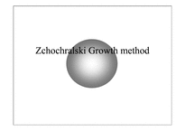
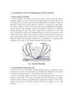
3. Monocrystal Silicon Growth
단결정 규소 봉으로 불뤼는 성장된 실리콘 단결정을 제작하기 위한 과정을 결정 성장이라고 합니다. 웨이퍼 제조에 사용된 실리콘 단결정 인곳(ingot: 금속 또는 합금을 한번 녹인 다음 주형에 흘려넣어 굳힌 것)의 성장을 위해 오늘날 가장 널리 이용되는 기술은 Czochralsik(CZ
To prevent silicon from agglomerating
→ should cool the solid quickly
Rapid cooling
→ large thermal gradient in crystal
Postulate K=20W/m K
Diameter of wafer: 10-20 cm
L (latent heat of fusion) = 340 cal/g
Temperature gradient in silicon CZ (dT/dx) : 100°C/cm
4. Dopant Barrier <불순물 장벽>
- 산화층이 실리콘 표면에서 성장하면 불순물 물질이 wafer로 들어가는 곳에 창을 생성시키기
위해서 Mask 개방으로 SiO2를 식각, 이때 산화물은 dopant의 확산으로부터
silicon의 표면을 보호.
- 선택적인 dopant의 도핑가능
5. 금속층 사이의 유전체
1. 단결정 성장
특수 공정을 이용해 웨이퍼 위에 전자회로를 새긴 후, 웨이퍼 위 집적회로(IC)를 각각 절단하면 IC칩이 되는 것인데요,
여기서, 웨이퍼(Wafer)란 반도체 집적회로를 만드는 중요한 재료로, 실리콘(Si), 갈륨 아세나이드(GaAs) 등을 성장시켜 얻은 단결정 기둥(Ingot)를 적당한 지름으로 얇게
4. 실험장비
① E-Beam Evaporator
PVD(Physical vapor deposition)의 한 방법으로 전자빔을 이용하여 박막을 형성하는 것이 E-Beam Evaporator이다. 그림5.는 E-beam장치의 구조도이다. 장치안의 필라멘트에 매우 높은 전압을 가하면 필라멘트에서 에너지를 가진 열전자들이 방출된다. 이 부분을 electron gun이라하고 여
② Thermal Evaporator
각종 금속(Au, Al, Ti, Cr, In, Ni)과 유전체(SiO2)의 박 막을 기판 위에 증착할 수 있는 장비이다. 진공도는 Torr까지 얻을 수 있다. 박막 증착시에는 박막 두께 측정 센서를 통해 박막의 두께를 확인하며 공정을 진행할 수 있다. 박막은 보통 0.5 Aring/sec ~ 1.0 Aring/sec의 증착 속도로 증착을 하
ML2 means the maskless lithography. It is necessary to refinement process. Described above, "double / mutiful patterning" in additional cost savings as an alternative to be appropriate. Nano devices with decreasing the size of the unilateral use light to produce a mask for the lithography process takes time and cost. Small production of nano scale patterning process is suitable, and the suitable